Reconstruction from LTE Mode to 4G & 5G Multi-Mode (L-Type Network)
The QCell (V4.0) networking solution is implemented in two phases: In phase 1, the B8200 and the B8300 can be connected, meaning that the LTE mode is commissioned. In phase 2, the NSA L-type network consisting of V9200+B8200/B8300 is supported, meaning that the LTE + 5G mode is commissioned.
The following describes the installation precautions during the upgrade from phase 1 to phase 2.
Engineering Reconstruction on the BBU Side
-
Install the V9200. Main control board: VSWc2; baseband board: VBPc5.
-
Check whether the boards of the B8200 meet the requirement. If not, replace the boards as required.
-
Main control boards: CCE1 and CCF0.
-
Baseband boards: BPN0_b, BPN0C, BPN2, BPQ0, and BPQ2.
-
FS boards; FS5C, FS5A, and CR0.
-
Check whether the B8200 is installed with the FS board. If not, install the board.
Optical Module Check and Rectification
As required by the FDD+5G NR multi-mode L-type networking scenarios, different optical interfaces of different devices have different optical module rates. You need to check the optical modules before reconstruction according to the following table to check whether the requirements are satisfied. If not, make rectifications as required.
Device |
Optical Interface |
Optical Module Rate |
Remarks |
B8200 |
OF0–OF5 of the FS board |
10G |
Interconnected with OF2, OF4, and OF6 of the VBPc5 board of the V9200. |
V9200 |
OF1, OF3, and OF5 of the VBPc5 board |
25G |
Interconnected with OF1 of the PB1124F. |
V9200 |
OF2, OF4, and OF6 of the VBPc5 |
10G |
Interconnected with OF0–OF5 of the FS board of the B8200. |
PB1124F |
OF1 and OF4 |
25G |
OF1 is interconnected with OF1, OF3, or OF5 of the VBPc5 board of the V9200. OF4 is used for cascading OF1 of the lower-level PB. |
PB1124F |
OF2 |
10G |
Interconnected with OF1–OF6 of the CFS board of the MA1020. |
PB1124F |
ETH1 to ETH8 |
10G |
Interconnected with ETH1 of the R8139. |
R8139 |
ETH1 |
10G |
Interconnected with ETH1–ETH8 of the PB1124F. |
MA1020 |
OF1 to OF6 |
10G |
Interconnected with OF2 of the PB1124F. |
Note:
-
If the PB1124F and the R8139 are connected through a CAT6a network cable, ETH1–EHT8 of the PB1124F and ETH1 of the R8139 do not need to be installed with optical modules.
-
If there are no RF feeders of other other manufacturers (without the MA1020) on the site, optical modules do not need to be installed for OF2 of the PB1124F.
Optical Fiber Connection Reconstruction
For a description of optical fiber connection reconstruction, refer to the following table.
Connection |
Connection Relationship (Before Re- construction) |
Connection Relationship (After Re- construction) |
Inter-BBU interconnection |
None. |
OF0–0F5 of the FS board of the B8200 are connected to OF2, OF4, and OF6 of the VBPc5 board of the V9200. |
BBU-to-PB1124F connection |
From OF0–OF5 of the FS board of the B8200 to OF1 of the PB1124F From OF0–OF5 of the baseband board of the BBU to OF1 of the PB1124F From OF7–OF12 of the CFS board of the MA1020 to OF1 of the PB1124F
|
OF1, OF3 and OF5 of the VBPc5 board of the V9200 are connected to OF1 of the PB1124F. |
BBU-to-MAU connection |
|
None. |
MAU-to-PB connection |
From OF7–OF12 of the CFS board of the MA1020 to OF1 of the PB1124F |
OF1–OF6 of the CFS board of the MA1020 are connected to OF2 of the PB1124F. |
Note:
In a QCell FDD+5G NR multi-mode L-type network, the VBPc5 board of the V9200 is used to cascade the FS board of the B8200, and is also connected to the PB1124F. Hardware limits: Ports 1–2, ports 3–4 and ports 5–6 must work in pairs, where ports 1, 3, and 5 are connected to the PB1124F and use 25 G optical modules, and ports 2, 4, and 6 are connected to the FS board of the B8200 and use 10 G optical modules. Port cross-connection modes, such as 1-4 and 3-6, are not supported. The following connection modes are not supported either: port 1 is used but port 2 is not used, port 3 is used but port 4 is not used.
For scenarios where feeders of other manufacturers are used, in LTE FDD networking mode, the BBU, MAU, and PB1124F use chain networking mode; the MAU is located between the BBU and the PB, and they are connected in series with optical fibers. In QCell FDD+5G NR multi-mode L-type networking mode, the MAU uses the star networking mode and is only connected to the OF2 interface of the PB1124F, without connecting to the BBU.
Clock Reconstruction
-
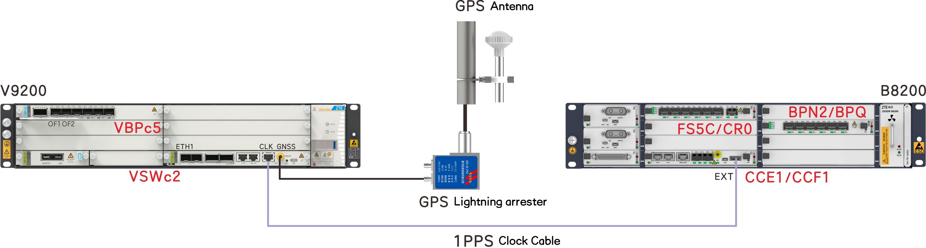
Change the GPS antenna feeder connection from the REF interface on the CC board of the B8200 to the REF interface on the VSW board of the V9200.
-
As the primary clock frame, the V9200 is connected to the GPS antenna feeder system, obtains clock information through the GPS, and converts it to an internal clock (which must be configured phase synchronization). Then, the clock signals are synchronously transmitted to the secondary clock frame.
As the secondary clock frame, the B8200 synchronizes the clock with the V9200 through a 1PPS clock cable, see the following figure.
The following figure shows the external view of a 1PPS clock cable.
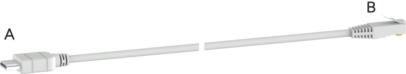
A 1PPS clock cable is 10 meters long. For a description of the interfaces and connections, refer to the following table.
Port Type |
End A: HDMI |
End B: RJ45 |
Connected to |
EXT interface of the CC board of the B8200 |
CLK interface of the VSWc2 board of the V9200 |